TiN coated conductive probes

TiN coated conductive probes
We would like to inform you that conductive TiN coated probes are coming back to the product line. Probe series - FMG01, NSG01, NSG10 - with hard and wear-resistant TiN coating are available for operating in any electrical AFM modes (C-AFM, PFM, EFM, KPFM, SSRM on polymers).
The main advantages of TiN coated probes are:
• Hard coating which stays stable at applied high voltages and flowing currents at the contact point ‘tip-sample’ which cannot be obtained with standard metal coated probes;
• High conductivity (close to metal conductivity);
• Typical curvature radius less than 35nm.
Titanium nitride (TiN) film provides excellent electrical conductivity, high voltage stability, wear resistance and conformal coating. The probes have ideal qualities for electrical AFM techniques like conductive AFM (C-AFM), piezoresponse force microscopy (PFM), electric field microscopy (EFM), etc.
TiN coating on highly doped silicon probes offers unparalleled sensitivity and stability while maintaining tip sharpness (35 nm) for consistent high resolution electrical characterization with long duration. TiN probes are quite stable at applied voltages up to ± 8V on a freshly cleaved HOPG with good wear resistance up to 50 scans on doped polysilicon sample.

TiN coated probes are also suitable for piezoresponse force microscopy for measuring of the electro-mechanical coupling behavior in variety of materials including ferroelectric, piezoelectric materials, biological samples, etc. They find applications in computer hard drive industry, nanolithography, material science and biomedical research.
TiN coatings on stiff (40N/m) and moderately stiff cantilevers (2-5 N/m) are also suitable for scanning spreading resistance microscopy (SSRM) applications on conductive polymer composite (CPC) materials. Other applications of TiN coated probes include non-contact electrical AFM techniques like EFM, surface potential measurements (Kelvin probe force microscopy, KPFM), etc.
The main advantages of TiN coated probes are:
• Hard coating which stays stable at applied high voltages and flowing currents at the contact point ‘tip-sample’ which cannot be obtained with standard metal coated probes;
• High conductivity (close to metal conductivity);
• Typical curvature radius less than 35nm.
Titanium nitride (TiN) film provides excellent electrical conductivity, high voltage stability, wear resistance and conformal coating. The probes have ideal qualities for electrical AFM techniques like conductive AFM (C-AFM), piezoresponse force microscopy (PFM), electric field microscopy (EFM), etc.
TiN coating on highly doped silicon probes offers unparalleled sensitivity and stability while maintaining tip sharpness (35 nm) for consistent high resolution electrical characterization with long duration. TiN probes are quite stable at applied voltages up to ± 8V on a freshly cleaved HOPG with good wear resistance up to 50 scans on doped polysilicon sample.

|

|
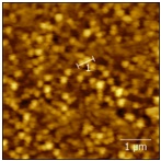
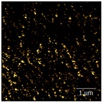
SSRM imaging of doped polysilicon sample with TiN coated probe.
Topography and current map.

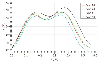
Plots of lateral profile of the same feature in different scans.
Profiles are very similar from 1 till 50 scan that show nondestructive properties
and long lifetime of TiN coated probe.
TiN coated probes are also suitable for piezoresponse force microscopy for measuring of the electro-mechanical coupling behavior in variety of materials including ferroelectric, piezoelectric materials, biological samples, etc. They find applications in computer hard drive industry, nanolithography, material science and biomedical research.
TiN coatings on stiff (40N/m) and moderately stiff cantilevers (2-5 N/m) are also suitable for scanning spreading resistance microscopy (SSRM) applications on conductive polymer composite (CPC) materials. Other applications of TiN coated probes include non-contact electrical AFM techniques like EFM, surface potential measurements (Kelvin probe force microscopy, KPFM), etc.
20.02.2016


